More powerful AI systems need more powerful chips, which means more fabs, more packaging capacity, and more sophisticated tools to run and monitor the manufacturing processes. The biggest concern of chip manufacturers is yield, the percentage of usable chips on a silicon wafer. Defects in semiconductor manufacturing are inevitable, and defect inspection is crucial for identifying the root cause of such faults. But modern chip packages become more and more complex, with multiple layers stacked in 3D. Each additional layer makes it harder to inspect a chip and localize defects.
A 2025 review from Arizona State University and the Fraunhofer Institute found that standard inspection methods force a trade-off: destructive techniques like cross-sectioning reveal defects but destroy the chip in the process, while non-destructive methods such as X-ray and acoustic microscopy struggle to resolve defects buried several layers deep without sacrificing depth or resolution. Once a defect sits three or four layers down, telling it apart from a routine manufacturing feature nearby becomes a matter of resolution most tools don't have. Yield takes the direct hit.
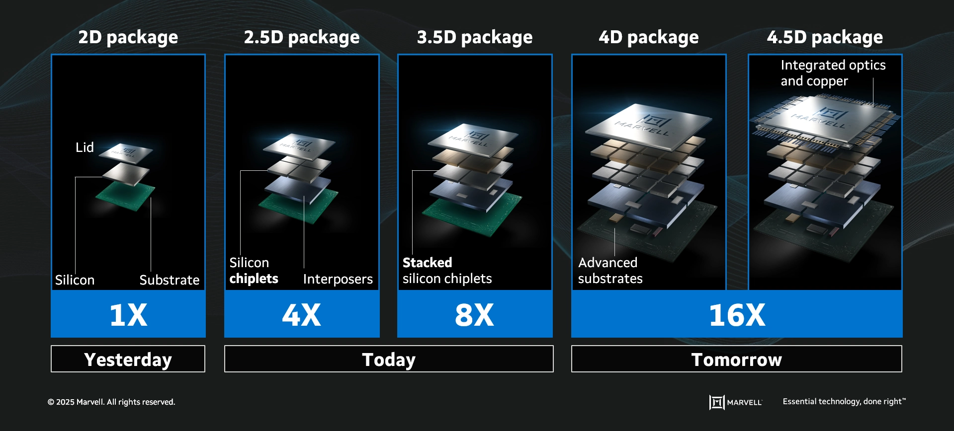
The global semiconductor market is projected to grow 18% to nearly $917 billion in 2026, and TSMC alone is guiding to $52-56 billion in capital spending for the year, up about 32% from an already-record 2025, with much of that capital aimed at advanced packaging, the technology that binds chiplets into a single AI accelerator. SEMI forecasts that advanced chipmaking capacity will grow 69% by 2028, with its CEO calling AI "a transformative force in the global semiconductor industry" driving that expansion.
More fabs and more advanced packaging both mean more chips that need inspecting, and the inspection market is growing on its own terms too: global spending on semiconductor inspection systems was valued at $5.2 billion in 2021 and is projected to reach $8.9 billion by 2031, a 5.4% annual growth rate. QuantumDiamonds points to industry estimates that a single percentage point of yield improvement can be worth millions of dollars a week for a high-volume device.
A single percentage point of yield improvement can be worth millions of dollars a week for a high-volume device.
Europe has an additional reason to care. The region produces less than 10% of the world's semiconductors today, and the European Chips Act has set a public investment target of more than €43 billion to double that share to 20% by 2030. Building new fabs is the visible part of that plan. Equipping them with tools that can see inside increasingly complex chips without destroying them is the less visible part, and it's where QuantumDiamonds sits.
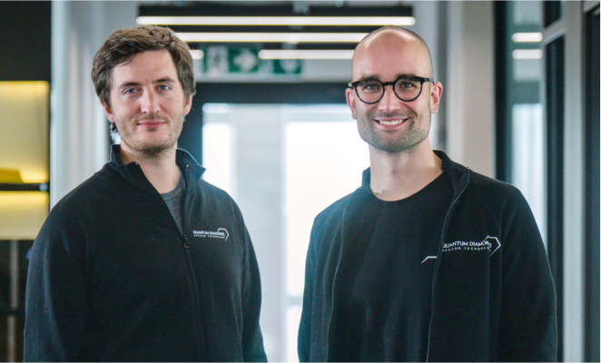
Fleming Bruckmaier, QuantumDiamonds' CTO, did his PhD in one of Europe's leading quantum sensing labs at the Technical University of Munich, under Prof. Dominik Bucher. He holds a Master's in Physics from ETH Zurich and a PhD in quantum sensing from TUM.
Kevin Berghoff, the CEO, met Fleming at TUM during his PhD, which he discontinued to found the company. He was at McKinsey for three years before, where he advised technology clients in the firm's Advanced Electronics practice across Europe and Asia.
They founded QuantumDiamonds in mid-2022, initially selling their diamond sensors to research labs. Kevin then worked through a wider set of possible markets before narrowing in on semiconductors. Conversations with chipmakers, including Munich-based Infineon Technologies, pointed to a specific gap in failure analysis: resolution, invasiveness, and speed, in that order. That gap became the company's focus.
The German Physical Society named QuantumDiamonds, together with TUM's School of Natural Sciences and Munich Quantum Valley, a recipient of its Technology Transfer Award for the transfer of the underlying quantum sensing research into an industrial product.
QuantumDiamonds' sensor is a diamond chip containing nitrogen-vacancy centers, atomic-scale defects created by removing two carbon atoms from the diamond lattice and replacing one with nitrogen. These defects respond to magnetic fields with enough sensitivity to detect the tiny fields generated by electrical current flowing through a chip's internal wiring.
The company places its diamond sensor on the chip package, illuminates it with a laser, and reads the resulting fluorescence to reconstruct the current flow inside the device, including layers buried under other layers. A short circuit, an open connection, or a leakage current all show up as a deviation from the expected current path, without cutting, grinding, or otherwise damaging the chip. According to the company's published technical specifications, the system resolves defects up to 100 times smaller than conventional inspection tools, with 100 to 1,000 times lower noise and 3 to 10 times higher sensitivity, and produces results in minutes rather than the hours or days a destructive physical failure analysis workflow requires.
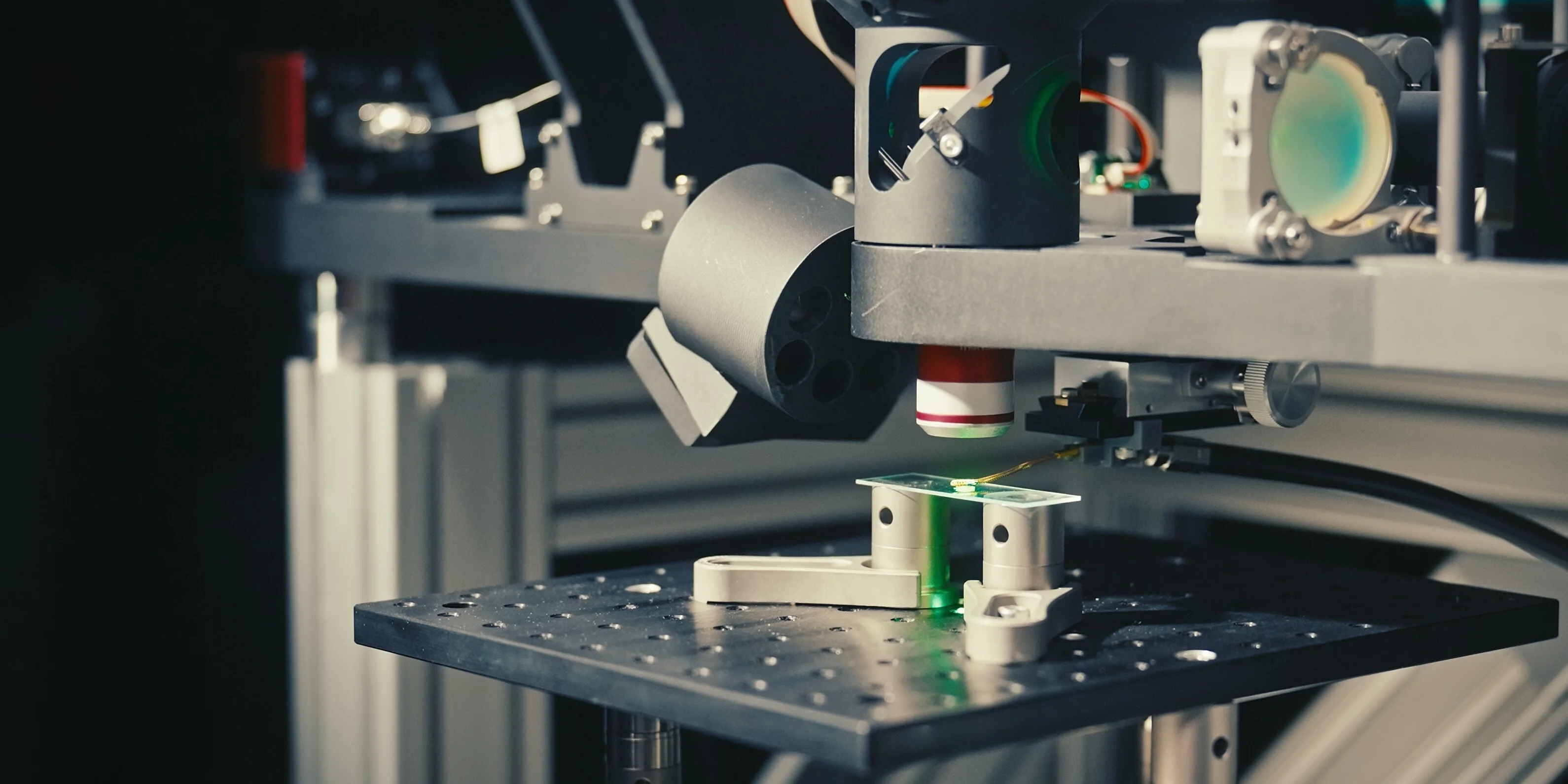
In a December 2025 study, QuantumDiamonds researchers demonstrated the technique on a commercial Apple A12 chip package, built on TSMC's Integrated Fan-Out Package-on-Package architecture. Working with a failure analysis lab in Taiwan, the team located a short circuit that conventional lock-in thermography could only partially localize, then confirmed the exact defect location with X-ray computed tomography. The magnetic imaging pinpointed a hairline crack in the package that other methods could only narrow down to a general area.
QuantumDiamonds says one U.S. chip designer had spent six weeks trying to debug a chip before the QDm.1 found the defect in under a minute.
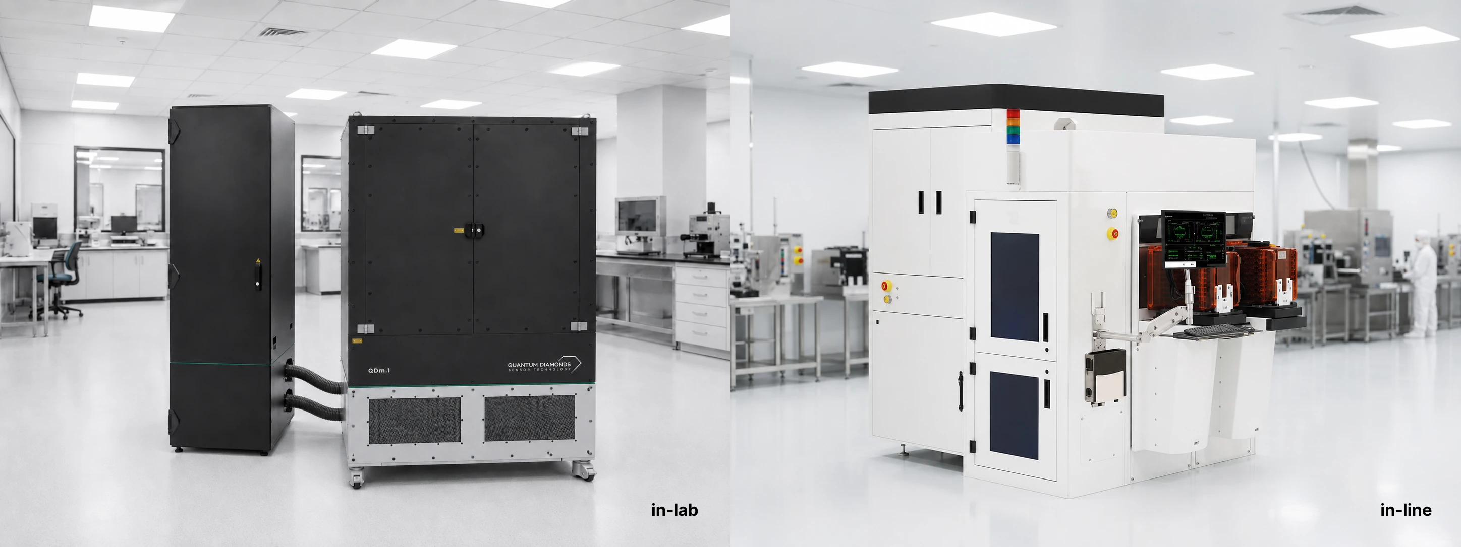
QuantumDiamonds raised a €7 million seed round in December 2023, led by IQ Capital and Earlybird, with First Momentum among the participating investors alongside Onsight Ventures, Creator Fund, UnternehmerTUM, the EIC Accelerator, and the Bavarian state. At the time, the team was testing its technology with some of the world's top semiconductor manufacturers. The company joined the Intel Ignite accelerator in April 2023 and launched its first commercial microscope, the QDm.0, in December of that year.
Since then, the number of engaged chipmakers has grown to 9 of the top 10 globally, with systems now running in Europe, the US, and Taiwan. Dr. Sean Shen, Director of Failure Analysis Engineering at iST in Taiwan, said the QDm.1 gives his engineers a fundamentally new way to interrogate advanced devices, non-destructively, in three dimensions, and at a speed that fits their workflow.
The number of engaged chipmakers has grown to 9 of the top 10 globally.
In July 2026, QuantumDiamonds closed a €91 million round: €15 million in new equity led by World Fund, with participation from Bayern Kapital and existing investors including First Momentum, plus €76 million in non-dilutive funding approved under the EU Chips Act. The public funding goes toward the €152 million production facility the company announced in Munich in December 2025, one of only 14 state aid decisions issued under the Act to date, where the first operational section is expected to open later this year. The company has over 60 full-time employees, serves customers on 3 continents, and plans to more than double its engineering team over the next 12 months.
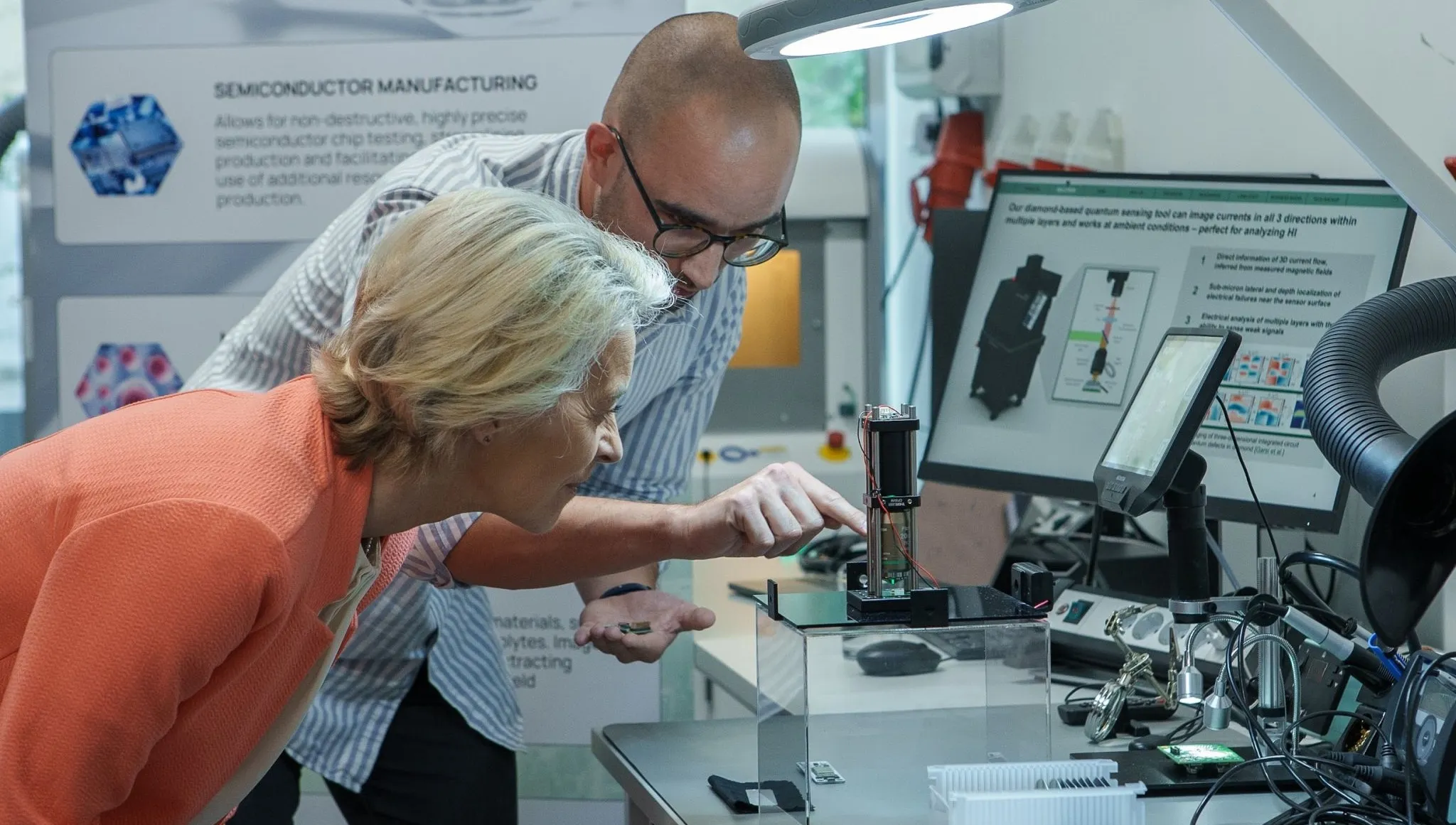
At pre-seed, QuantumDiamonds combined the two things we look for in a deep tech team: a founder who deeply understands the physics and a founder who can sell it, a pairing our own research shows is rarer than it should be. Fleming had already built a working sensor with sensitivity advantages over existing tools. Kevin tested the technology against several possible markets and validated it directly with the chipmakers who'd eventually become customers.
AI demand is pushing chipmakers toward more advanced packaging, and every layer they add makes a chip harder to test without destroying it. QuantumDiamonds sits right at the intersection of that growing problem and one of the strongest quantum sensing labs in Europe, with a sensor built to see what acoustic and X-ray methods can't.
Three years on, that combination has turned a lab sensor into a product with traction across the world's largest chip companies, and QuantumDiamonds into one of the fastest-growing, best-funded early-stage semiconductor startups in Europe.